
FAQs2024-06-21T06:05:11+00:00

What Is Surface Mounted Technology and How Does It Work?

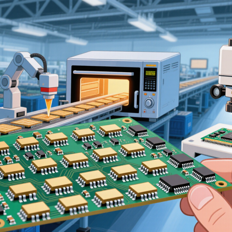
Surface Mounted Technology has transformed modern electronics by placing components directly onto a printed circuit board’s surface. Unlike through-hole assembly, it needs no drilled component leads. Tiny resistors, capacitors, and integrated circuits sit on copper pads, then pass through solder paste printing, automated placement, and controlled reflow. The result can be a compact board, often thinner than a finger.

Industry data shows why this method matters. Fortune Business Insights estimates that the surface-mount technology equipment market could grow from about USD 5.1 billion in 2023 to USD 8.4 billion by 2030. IPC’s electronics industry reports also continue to identify supply-chain pressure, skilled labor shortages, and quality control as major manufacturing concerns. Estimates vary between reports. That difference deserves attention.

As electronics manufacturing consultant Bob Willis explains, “Process control is the key to consistent soldering.” His point is practical. A misplaced component, a blocked stencil aperture, or a poorly controlled reflow profile can weaken an entire assembly. I have found that the impressive speed of Surface Mounted production can hide fragile details. The machine may place thousands of components per hour, but reliability still depends on paste volume, pad design, component moisture, and inspection discipline.

This guide explains what Surface Mounted Technology is, how each production stage works, and where defects commonly appear. It also examines automated optical inspection, solder joint reliability, and design-for-manufacturing decisions. The process looks simple from a distance. It is not.
What Is Surface Mounted Technology and How Does It Work?

Surface-Mount Technology: Definition, Scope, and 0.4 mm-Pitch Assemblies

Surface-Mount Technology: Definition, Scope, and 0.4 mm-Pitch Assemblies

Surface-Mount Technology places electronic components directly onto printed circuit board pads. Unlike through-hole assembly, it needs no drilled lead holes for most parts. The process usually includes solder-paste printing, component placement, reflow heating, inspection, and electrical testing. According to a 2024 market assessment by Grand View Research, the global SMT equipment market was valued at approximately USD 5 billion in 2023. That figure reflects expanding demand for compact, automated electronics.

The scope is broader than small consumer devices. Automotive controllers, medical instruments, industrial sensors, and communication modules all use SMT assemblies. At 0.4 mm pitch, adjacent component leads sit only 0.4 millimeters apart. Tiny misalignment matters. IPC assembly guidance emphasizes controlled paste volume, pad design, thermal profiling, and inspection for fine-pitch reliability. In production, automated optical inspection can detect bridging, skew, and insufficient solder, while X-ray inspection helps reveal hidden joints beneath area-array packages. The IPC 2023 Electronics Industry Sentiment Report also identified skilled labor and supply-chain pressure as continuing manufacturing concerns. That matters because advanced placement equipment cannot replace sound process decisions.

From practical experience, 0.4 mm assembly often fails at the paste-printing stage, not during placement. Stencil thickness, aperture reduction, board warpage, and humidity can change the result. Small details dominate. A clean laboratory trial may still perform poorly in volume production. Engineers should challenge their first process window, measure defects by location, and allow room for design corrections. Perfect repeatability is an aspiration, not an assumption.

PCB Preparation: Solder-Paste Printing with 50–150 µm Stencils

Surface-mounted technology places components directly onto copper pads, but reliable assembly starts before placement. Solder-paste printing controls the first critical deposit. A stainless-steel stencil, commonly 50–150 µm thick, transfers paste through laser-cut apertures. The printed volume equals aperture area multiplied by stencil thickness. For example, a 0.30 mm square aperture with a 100 µm stencil deposits about 9 nanolitres before transfer losses.

Small details matter. The stencil must sit flat against the PCB. Excessive separation can smear paste between pads. Too little pressure may leave incomplete deposits. IPC-7525C recommends designing apertures around pad geometry, paste release, and component pitch. Its guidance supports practical control rather than a universal stencil thickness. A 50 µm stencil may suit fine-pitch components, while 150 µm can provide more volume for larger joints. Thicker is not automatically better.

Industry data reinforces the risk. The 2024 electronics manufacturing outlook from the Global Electronics Association identifies miniaturisation and yield control as continuing production pressures. IPC solder-paste guidance also treats deposit volume, alignment, and paste condition as measurable process variables. In production, solder-paste inspection should check area, height, and volume after printing. A common target is around 100% of the programmed deposit, with process limits often set near ±10%, depending on the assembly design. That tolerance deserves review. It may be too generous for 0.4 mm-pitch parts. Operators should verify it with real boards, not assumptions. Fresh paste, stable room temperature, and regular stencil cleaning remain essential. Small errors accumulate quickly.

Pick-and-Place Assembly: 01005 Components and 100,000 CPH Placement Rates

Surface Mounted Technology places electronic components directly onto copper pads on a printed circuit board. Solder paste holds each part before reflow heating creates permanent joints. The process saves space and supports dense, lightweight assemblies.

Pick-and-place machines can advertise placement rates near 100,000 components per hour. That figure describes ideal movement, not every production run. Feeder changes, board size, component spacing, and inspection pauses reduce the real rate. A balanced line may deliver less, but with better stability.

Tiny 01005 components measure about 0.4 by 0.2 millimeters. They demand accurate stencil printing, controlled paste volume, and reliable vision alignment. Even slight pad contamination can cause opens or bridging. During setup, engineers usually check paste deposits with three-dimensional inspection before full production. This catches problems early.

The machine must also manage fragile feeders and rapid acceleration. A component can rotate, shift, or remain trapped in the tape pocket. That happens.

Experienced technicians adjust placement force, nozzle selection, and conveyor support for each board design. However, speed alone is a weak performance measure. High throughput with poor first-pass yield creates hidden rework and wasted material. I have found that small 01005 parts often expose weaknesses in cleaning, humidity control, and operator discipline. The process is precise, but never completely forgiving.

What Is Surface Mounted Technology and How Does It Work? - Pick-and-Place Assembly: 01005 Components and 100,000 CPH Placement Rates

Surface-Mount Technology and Pick-and-Place Assembly Data Overview
Data Dimension Typical Value or Range What It Means in Practice Key Process Consideration
Surface-Mount Technology (SMT) Electronic components are mounted directly onto the surface of a printed circuit board (PCB). Components usually do not require leads to pass through drilled holes, allowing higher component density and automated assembly. PCB land patterns, solder-paste deposits, component orientation, and thermal profiles must be designed for surface mounting.
Common SMT Component Types Chip resistors, chip capacitors, diodes, transistors, integrated circuits, connectors, and modules. Components are supplied mainly on reels, trays, or tubes and are fed into automated placement equipment. Each package requires a compatible feeder, nozzle, vision-recognition setting, and PCB footprint.
01005 Component Size Approximately 0.4 mm × 0.2 mm “01005” commonly refers to the imperial package designation for an extremely small passive component. The approximate metric dimensions are 0.4 mm × 0.2 mm. Handling requires precise tooling, stable component presentation, accurate fiducials, controlled solder-paste printing, and high-quality inspection.
Other Common Passive Package Sizes 0201: approximately 0.6 mm × 0.3 mm; 0402: approximately 1.0 mm × 0.5 mm; 0603: approximately 1.6 mm × 0.8 mm. Smaller packages save board space, while larger packages are generally easier to print, place, inspect, and rework. Package selection should balance electrical performance, available board area, assembly capability, inspection needs, and serviceability.
Solder-Paste Printing Stencil apertures commonly range from fractions of a millimeter to several millimeters, depending on the component footprint. A stencil printer deposits solder paste onto PCB pads before component placement. Paste volume, aperture design, alignment, separation speed, cleaning frequency, and paste condition strongly influence solder-joint quality.
Pick-and-Place Function Components are picked from feeders or trays, optically checked, rotated, and positioned on solder-paste-covered PCB pads. The machine converts a placement program into controlled X-Y-Z and rotational movements. Feeder setup, nozzle condition, component recognition, board support, and placement sequencing affect throughput and accuracy.
Placement Rate Up to approximately 100,000 components per hour on high-speed systems under ideal conditions. 100,000 components per hour equals about 27.8 theoretical placements per second. Actual line output is normally lower because of component mix, feeder changes, PCB size, inspection, stoppages, nozzle changes, and other production constraints.
Placement Rate Measurement Components per hour (CPH), also called placements per hour. CPH is a machine-speed indicator rather than a guaranteed finished-board production rate. Use actual placements per board, cycle time, changeover time, uptime, and first-pass yield to estimate practical capacity.
Placement Accuracy High-precision equipment may specify accuracy in the tens of micrometers, depending on the machine, component size, and measurement conditions. Accuracy describes how closely a component is placed to its programmed position. Accuracy is influenced by board expansion, fiducial quality, machine calibration, nozzle wear, component tolerances, and placement force.
Reflow Soldering Most SMT assemblies use a controlled heating profile with preheat, soak, reflow, and cooling stages. Solder paste melts during the reflow stage and forms electrical and mechanical connections between components and PCB pads. The profile must match the solder alloy, PCB mass, component limits, and assembly requirements while avoiding overheating or insufficient wetting.
Lead-Free Solder Temperature Lead-free solder alloys commonly reflow at peak temperatures around 230°C to 250°C, depending on alloy and process specification. The selected alloy determines the required thermal profile and the time above liquidus. Always follow the solder-paste manufacturer’s profile limits and the temperature sensitivity limits of the components and PCB.
Inspection Methods Automated optical inspection (AOI), solder-paste inspection (SPI), and X-ray inspection. SPI checks paste deposition; AOI checks visible placement and solder features; X-ray can inspect hidden joints such as bottom-terminated packages. Inspection coverage should be selected according to package type, defect risk, product reliability requirements, and applicable quality standards.
Typical SMT Process Sequence PCB loading → solder-paste printing → SPI → component placement → reflow soldering → AOI/X-ray → electrical test. The sequence combines material deposition, automated assembly, thermal bonding, inspection, and functional verification. Process controls and traceability at each stage help identify defects early and reduce rework.
Main Benefits High component density, automated production, repeatable placement, reduced assembly labor, and suitability for compact products. SMT supports smaller and lighter electronic assemblies with efficient high-volume manufacturing. Benefits depend on appropriate design-for-manufacturing rules, stable materials, equipment capability, and process control.
Main Limitations Very small components can be difficult to handle, inspect, repair, and rework; thermal and mechanical constraints also apply. Miniaturization does not automatically improve manufacturing yield or serviceability. Use suitable package sizes, component spacing, test access, board support, and rework methods for the intended production volume.

Note: Values shown are general industry figures and typical engineering ranges. Actual performance depends on equipment configuration, PCB design, component mix, materials, process settings, and production conditions.

Reflow Soldering: 8–12 Thermal Zones for Controlled Joint Formation

Surface Mounted Technology places electronic components directly onto circuit board pads. Reflow soldering then forms reliable joints through controlled heating. An oven with 8–12 thermal zones provides the control needed for this process. Each zone adjusts temperature, airflow, or heating intensity. The board travels steadily through these stages. Not quite simple. Real profiles depend on board thickness, copper weight, component size, and solder paste chemistry.

Preheat zones raise the board temperature gradually and reduce thermal shock. Soak zones help equalize temperatures across dense and open areas. This stage also activates the solder paste flux. The peak zone melts the solder and allows wetting across each pad. Time above liquidus must remain within the paste supplier’s process window. Cooling zones then lower the temperature at a controlled rate. Too rapid cooling can stress joints or components. Too slow cooling may produce coarse solder structures. That matters.

A reliable setup begins with measurement, not guesswork. Technicians attach thermocouples near large ground planes, small components, and thermal edges. These readings reveal whether the center and edges actually share a usable profile. One profile rarely suits every board design. A temperature curve that looks acceptable on paper can still create insufficient wetting or voiding. Adjustments should be small and recorded carefully. Sometimes, an operator changes airflow when the real problem is conveyor speed. That mistake is easy to make. Inspection should combine profile data, visual checks, and cross-section analysis when joint quality remains uncertain.

Inspection and Reliability: SPI, AOI, X-Ray, and IPC-A-610 Class Criteria

Surface-mounted technology places components directly onto printed circuit boards, enabling compact and automated assembly. Inspection protects that speed from becoming hidden risk. Solder paste inspection, or SPI, measures paste height, area, volume, and alignment before components are placed. A small paste shortage can later become an open joint. Excess paste may create bridging.

Automated optical inspection, or AOI, checks component presence, polarity, placement, and visible solder shapes. It works well after reflow, but it cannot see every joint. X-ray inspection helps examine hidden connections beneath packages, including voids, bridges, and incomplete solder joints. In production reviews, I have found that one method rarely tells the whole story. A clean image can still hide a weak connection.

IPC-A-610 class criteria provide a common basis for judging assembly acceptability. Class 1 supports general products, while Class 2 requires dependable performance for dedicated service. Class 3 demands tighter control for high-performance or critical equipment. The selected class should match the product’s real operating risks, not convenience. Inspection records should include equipment calibration, defect images, repair history, and lot traceability. Sampling can reduce cost, yet it may miss an isolated failure. That limitation deserves honest review. Human judgment also matters when evidence falls between clear acceptance and rejection.

Go to Top